Concept explainers
Videos
(a)
Write the nodal equation of the circuit.
(a)
Answer to Problem 45E
The nodal equation of the circuit at node voltage
Explanation of Solution
Calculation:
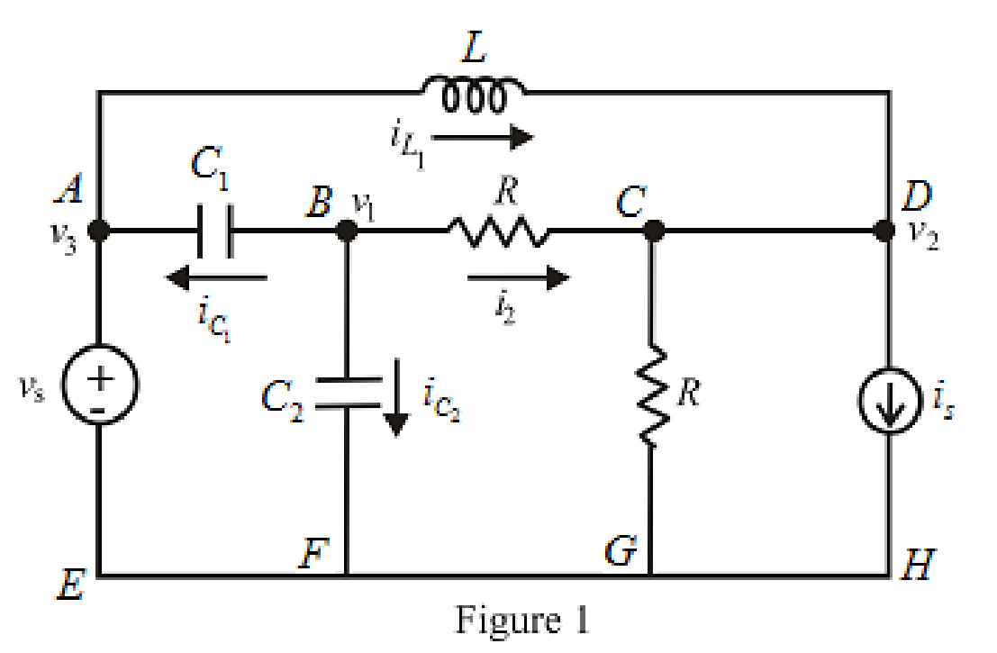
The redrawn circuit is shown in Figure 1.
Here,
The expression for the current across the inductor is,
Here,
The expression for the current across capacitor is,
Here,
The expression for the nodal analysis at node
Rearrange equation (3),
The voltage at node voltage
Substitute
The expression for the nodal analysis at node voltage
The node voltage across resistance
Rearrange equation (7),
Conclusion:
Thus, the nodal equation of the circuit at node voltage
(b)
Write the mesh equation of the circuit.
(b)
Answer to Problem 45E
The mesh equation of the circuit in loop
Explanation of Solution
Calculation:
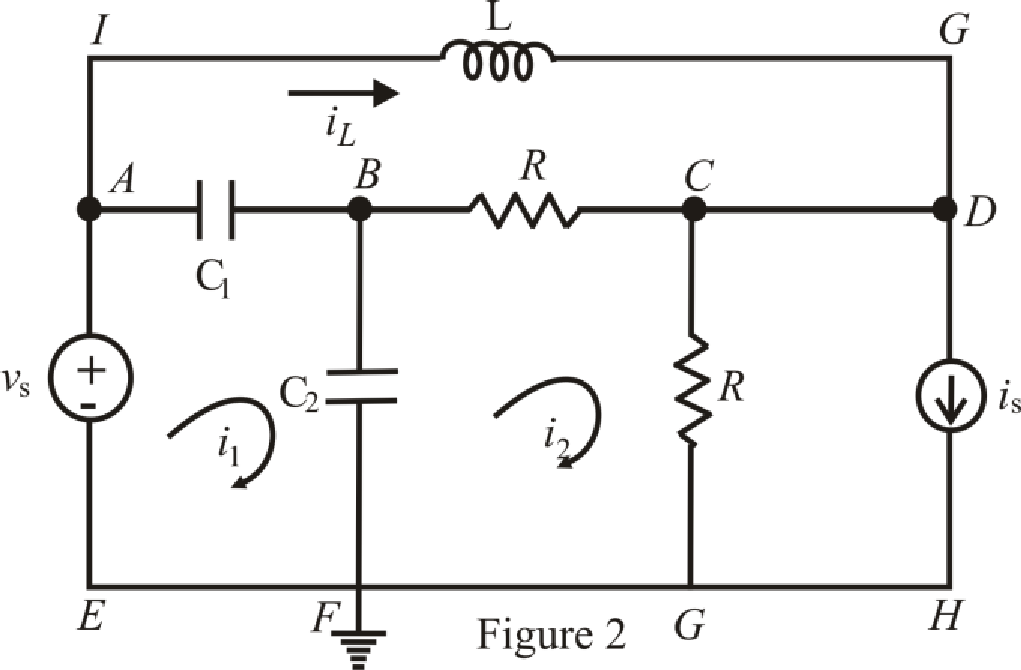
The redrawn circuit is shown in Figure 2 as follows,
Refer to the Figure 2,
The voltage at node voltage
The expression for mesh equation in loop
Here,
Substitute
The expression for mesh equation in loop
Substitute
The expression for mesh equation in loop
Conclusion:
Thus, the mesh equation of the circuit in loop
Want to see more full solutions like this?
Chapter 7 Solutions
Loose Leaf for Engineering Circuit Analysis Format: Loose-leaf


- . Calculate v, and i̟ for each of the circuits depicted in Fig. 7.48, if i, = 1 mA and v, = 2.1 V. iL 14 kN is 12 nH 4.7 kN llarrow_forwardElectromagnet, picture 2 is an example of doing Practice Exercise 7.7, thank you in advance.arrow_forwardReduce the circuit depicted in Fig. 7.58 to as few components as possible. 2 V + R W ww R R M FIGURE 7.58 с R + Vx CL ell R мее L Carrow_forward
- Using Thevenin's Theorem, rewrite the physical network from Figure 7 as an equivalent Thevenin Network, i.e. express Veq as a function of V₁ and V₁ and Req as a value. If the voltage sources Vo and V₁ are the outputs of digital pins on an Arduino (i.e. 0 volts or 5 volts), what are the four possible values of Veq? + Vol + 2R Physical circuit 2R VO m 3.3ΚΩ m t Figure 7: Resistor Network for Thevinin's Theorem Using Thevenin's Theorem rewrite Vout from Figure 8 as a function of vo through v3. We will consider these voltages to be the inputs of this circuit. Since they are inputs, they can also be thought of as implicitly declared volt- age sources. You may expand vo through v3 as voltage sources (referenced to ground) to make the circuit more clear. For analysis, you will find it most useful to break the circuit and cascade Thevenin's Theorem from the left most point to the right most point. Note the pattern that appears with each additional R-2R m R Vout section in your prelab. If the…arrow_forward15. For the network of Fig. 7.78: a. Determine the current I. b. Find V V = +9 V R2 R3 2 = -19 V %3D FIG. 7.78 Problem 15.arrow_forwardElectrical engineering A mesh collider a) is as accurate as the triangle count on the mesh b)is the variable optiom for complex meshes such as player characters c)is the only way to get headshots to work d)is faster than a box colliderarrow_forward
- Calculate v₁ and it for each of the circuits depicted in Fig. 7.48, if is = 1 mA and vs 2.1 V. = Vs is + 4.7 ΚΩ M (a) 4.7 ΚΩ. (c) 12 nH iL 12 nH VL is Vs + 4.7 ΚΩ 14 ΚΩ M (b) 4.7 ΚΩ (d) iL 12 nH iL m +51 12 nH 14 ΚΩ ww VL ell +51 VLarrow_forwardSolution: Redrawing the network after combining series e yields Fig. 7.23, and Is 16 24 k) 24 kN R6 12 kN R1,2,3 R4 Is E=72 V R7 R8.9 V7 9 kS R5 12 kN 9 kΩ Is 16 FIG. 7.23 Network of Fig. 7.22 redrawn.arrow_forwardPROBLE M 7.15 Determine VOUT versus vIN for the circuit shown in Figure 7.8 Assume that the MOSFET operates in saturation and is characterized by the paramete K and VT. What is the value of VOUT when VỊN = 0? PROBLEM 7.16 Determine vo versus vị for the circuit shown in Figure 7.8 Assume that the MOSFET operates in saturation and is characterized by the paramete K and VT. What is the value of vo when vj = = 0?arrow_forward
- Calculate vL and ir for each of the circuits depicted in Fig. 7.48, if i, = 1 mA and v, = 2 V. 4.7 kΩ 14 kΩ 12 nH 12 nH 4.7 kN elearrow_forwardS0. Although the readings of Fig. 7.99 initially suggest that the network is behaving properly, detemine a possible cause for the undesirable state of the network. 20 V 2.2 k2 330 k2 IDss = 10 mA Vp = -6 V 3.7 V 6.25 V 75 kN 1 k2 FIG. 7.99 Problem 30.arrow_forward2.15 Design Problem for DC Circuits EXAMPLE 7.16 The levels of Vps and Ip are specified as Vps = VDD and Ip = ID(on) for the network of Fig. 7.54. Determine the levels of Vpp and Rp. VDD 10 ΜΩ RD VGS(on) = 6 V ID(on) = 4 mA VGS(Th) = 3 V FIG. 7.54 Figure 2.14 Example for Design Problemarrow_forward
 Introductory Circuit Analysis (13th Edition)Electrical EngineeringISBN:9780133923605Author:Robert L. BoylestadPublisher:PEARSON
 Delmar's Standard Textbook Of ElectricityElectrical EngineeringISBN:9781337900348Author:Stephen L. HermanPublisher:Cengage Learning
 Programmable Logic ControllersElectrical EngineeringISBN:9780073373843Author:Frank D. PetruzellaPublisher:McGraw-Hill Education
 Fundamentals of Electric CircuitsElectrical EngineeringISBN:9780078028229Author:Charles K Alexander, Matthew SadikuPublisher:McGraw-Hill Education
 Electric Circuits. (11th Edition)Electrical EngineeringISBN:9780134746968Author:James W. Nilsson, Susan RiedelPublisher:PEARSON
 Engineering ElectromagneticsElectrical EngineeringISBN:9780078028151Author:Hayt, William H. (william Hart), Jr, BUCK, John A.Publisher:Mcgraw-hill Education,