Concept explainers
Videos
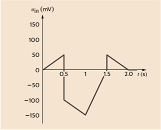
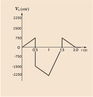
An amplifier has a gain of 15 and the input waveform shown in Fig. P4.1. Draw the output waveform.
To draw:
The output waveform using input waveform and gain of the amplifier.
Explanation of Solution
Given:
Amplifier has a gain of 15 and input waveform shown below.
Calculation:
For an amplifier, output voltage is product of gain and its input voltage.
In the given figure, calculate the output voltage by the above formulae at different time to form a graph.
At
At
At
At
At
The output waveform for the given input is shown below.
Want to see more full solutions like this?
Chapter 4 Solutions
Basic Engineering Circuit Analysis


- 4.37 Find the range of Rf for which the op amp in the circuit of Fig. P4.37 does not saturatearrow_forward4.31 Determine the current io flowing into the op-amp of thecircuit in Fig. P4.29 under the conditions Vs = 0.5 V, V0 = 0 V,and RL = 10 k Ohmsarrow_forwardProblem 4.17: You have access to resistors with values 1 k2, 1.5 kn, and 5.0 k2. You have a voltage signal from a transducer with a maximum voltage of 0.2 V. Using a noninverting op amp configuration, what maximum output voltages could you provide with the combinations of these resistors? Sketch your op amp circuit options.arrow_forward
- The circuit shown in Fig. 4 provides transfer characteristics with +7.5 V levels at the output vo. When v 0 V, a current of 0.5 mA flows in the feedback resistor (R2) and a current of 1.0 mA flows through the zener-diodes. Assume that the output saturation levels of the op-amp are ±12.0 V, the forward-drop voltage of the zener-diode is 0.7 V, and the value of R, is equal to R2. a) Specify the zener-voltages of the zener diodes. b) Find the values of all resistors. R2 R1 R Z Z, Fig. 4arrow_forward(Q4.1) Determine the voltage gain G1=vO1/vS: (Q4.2) Determine the voltage gain G2=vO/vS:arrow_forwardQ4: Consider the uA741C-based op-amp amplifier circuit shown below; The input voltage, Vi, is 2.5 volts. R2 is 5,000 ohms and RI is 1,000 ohms : R2 vo • What is the name of the circuit? • What is the value of the voltage at the negative input of the op-amp? • What is the value of the current through the 1 k2 resistor, in?arrow_forward
- Find the voltage gain of the op-amp circuit shown in Fig. P4.30. (R1-20 KQ, R2-84 k0, R3-4 k0, R4-30 KQ) V₁ R1 ww Figure P4.30 R2 ww R3 ww R4 Varrow_forwardQ4: Design a buck-boost converter to provide an output voltage 12V from a source that varies 'between 10V-16V. Given the load resistor is 10 ohm. assuming the frequency is 50 KHz and the output voltage ripple is 1.5% Specity: a. The duty ratio. b. The value of inductor. c. The value of capacitor. Note: Determine the values of inductor and capacitor with D1 only.arrow_forward4.17 Using the ideal op-amp assumptions, determine I₁, I₂, and I3 in Fig. P4.17. 1 mA Figure P4.17 m R₁ 1₁ 13 12 ww R₂ Voarrow_forward
- Figure QI shows the circuit diagram of a "Logarithmic Amplifier". In this circuit the feedback resistor of a normal inverting amplifier is replaced by a silicon diode. Since the current flowing through the diode increases exponentially with the voltage across the diode, the voltage across the diode will be proportional to the logarithm current flowing through it. Hence the output of the circuit is proportional to the logarithm of the input voltage. QI DI RIN Al Figure QI The current flowing through a diode is given by the Shock' y Diode Equat n: 1,=1, (e" =1) where , is the current flowing through the diode g is the charge on the electron (given at the back of the examination sheet) V, is the voltage across the diode K, is Boltzmann's constant (given at the back of the examination sheet) Tis room temperature (given at the back of the examination sheet) Given that /,> 1, an approximate expression for V, as a function of I, is Continued overleaf Page 2 of 9 QI (a) 0) Neglecting any input…arrow_forwardP4.8 Extreme temperature changes result in many failures of electronic circuits [1]. Temperature control feedback systems reduce the change of temperature by using a heater to overcome outdoor low temperatures. A block diagram of one system is shown in Figure P4.8 D. The effect of a drop in environmental temperature is a step decrease in Ta(s). The actual temperature of the electronic circuit is Y(s). The dynamics of the electronic circuit temperature change are represented by the transfer function. 200 G(s): s2 + 25s + 200 (a) Determine the sensitivity of the system to K. (b) Obtain the effect of the disturbance Ta(s) on the output Y(s). T(8) Heater control Electronic circuit + K R(s) G(s) Y(s) 0.1s + 1 Figure P4.8 Temperature control system.arrow_forwardQuestion 1 A class A output stage is supplied by Vcc = 10 V and biased with current source producing I = 100 mA. When a signal is applied at its input, a resulting 8-Vpp signal is formed across a 100-2 load. The power conversion efficiency of this amplifier is: O4% 16% 25% 32%arrow_forward
 Introductory Circuit Analysis (13th Edition)Electrical EngineeringISBN:9780133923605Author:Robert L. BoylestadPublisher:PEARSON
 Delmar's Standard Textbook Of ElectricityElectrical EngineeringISBN:9781337900348Author:Stephen L. HermanPublisher:Cengage Learning
 Programmable Logic ControllersElectrical EngineeringISBN:9780073373843Author:Frank D. PetruzellaPublisher:McGraw-Hill Education
 Fundamentals of Electric CircuitsElectrical EngineeringISBN:9780078028229Author:Charles K Alexander, Matthew SadikuPublisher:McGraw-Hill Education
 Electric Circuits. (11th Edition)Electrical EngineeringISBN:9780134746968Author:James W. Nilsson, Susan RiedelPublisher:PEARSON
 Engineering ElectromagneticsElectrical EngineeringISBN:9780078028151Author:Hayt, William H. (william Hart), Jr, BUCK, John A.Publisher:Mcgraw-hill Education,