
Videos
(a)
To construct: The table for the state of each transistor.
To find: The output voltage
(a)
Answer to Problem 16.62P
The value of the output voltages is obtained and is shown in Table 2
Explanation of Solution
Calculation:
The given diagram is shown in Figure 1
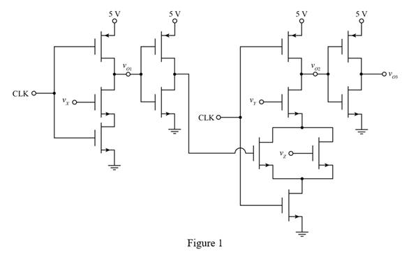
The given table is shown in Table 1
Table 1
| State | CLK | |||
For state 1
The input clock signal input X, Y and Z are at logic zero and the logic function of the output voltage
Substitute
From the circuit the NMOS device with the input
The expression for the logic function of the output voltage
Substitute
The logic function of the output voltage
Substitute
For state 2.
All the inputs are at logic 1.
Substitute
Substitute
Substitute
For state 3.
All the inputs are at logic 0.
Substitute
Substitute
Substitute
For state 4.
The input clock,
Substitute
Substitute
Substitute
For state 5.
All the inputs are at logic zero.
Substitute
Substitute
Substitute
For state 6.
The input clock,
Substitute
Substitute
Substitute
The table for the state of the transistors and the output voltage is shown in table below.
The required table is shown in Table 2
Table 2
| State | CLK | ||||||
The table for the state of the transistor is shown below.
Conclusion:
Therefore, the value of the output voltages is obtained and is shown in Table 2
(b)
The logic function that the circuit implements.
(b)
Answer to Problem 16.62P
The logic that the circuit performs is
Explanation of Solution
Calculation:
The expression for the output voltage
Substitute
Conclusion:
Therefore, the logic that the circuit performs is
Want to see more full solutions like this?
Chapter 16 Solutions
Microelectronics: Circuit Analysis and Design


- Using the sine PWM method with the full bridge inverter below, it is desired to generate a voltage of 50 Hz on the serial RL load. A voltage of 120 V DC is applied to the input of the inverter circuit. Amplitude modulation rate ma -0.9 and frequency modulation rate mf -19. The resistance of the series RL load is 15 OHM and the coil inductance is 40 mH. a) What is the power drawn by the load resistor?b) What is the total harmonic distortion value (THD) of the load current?arrow_forwardQuestion- A single phase full bridge inverter controls the power in a resistive load by uniform multiple pulse modulation. The frequency of triangular carrier wave is 1kHz and inverter reference wave frequency is 125Hz. If the total pulse width is 120°, find the width of each pulse?arrow_forward6- Design a logic cct using NAND gate and convert BCD code to Excess-3code.arrow_forward
- Q1) List the main internal elements of a microcontroller. And explain the function of each of them. Q2) What is the difference between the Von-Neuman Microcontroller Architecture and Harvard Microcontroller Architecture. Q3) Compare between the (EEPROM) and the Non-Volatile RAM - (NVRAM). Q4) What is the term “Complex Instruction Set Computer(CISC)” mean in the Microcontroller Architecture.arrow_forwardUsing the sine PWM method with the full bridge inverter below, it is desired to generate a voltage of 50Hz on the series RL load. A voltage of 120 V DC is applied to the input of the inverter circuit. Amplitude modulation rate ma = 0.9 and frequency modulation rate mj = 19. The resistance of the series RL load is 15 ohms and the coil inductance is 40 mH. What is the total harmonic distortion value (THD) of the power drawn by the load resistor and the load current?arrow_forward(a) Figure Q.4 (a) shows a combinational logic cireuit with output, Z and Table Q.4(a) depicts the delay for each logic gate in nanoseconds (ns). Determine the critical path and critical path delay in nanoseconds (ns). В Figure Q.4(a) Table Q.4 (a) Logic Gate NOT Delay (ns) 4 OR 8 AND 16 NAND 12 NOR 10 XOR 28 XNOR 32arrow_forward
- Draw the figure for memory segments with 8086 microprocessor software model. Explain the logical address structure used for each segment (Explain which registers are used in logical address presentation of each segment; segment address : offset address). Give an example solution to find the physical address in a segment from the logical address for 8086 microprocessor.arrow_forwarda) A standard TTL inverter gate is shown in the figure. The supply voltage is 5V. Calculate the output voltage for both logic low and logic high input cases assuming input voltages respectively as 0.11V and 4.2V. Br= 130; BR = 0.24. You can make approximations when needed. Br = IcIs active region; BR = IE/ls inverse active region b) Assume you connect a resistor of 1.8K to the output of the circuit when the output is at logic high. What will be the change in the output voltage? 1302 R3 1.6k2 R, 4k2 Input o T, Output T, V, V. IkQ R,arrow_forwardQUESTION TWO A single-phase asymmetrical semiconverter feeds an RL load with R = 10 N and a large L so that load current is level. The source voltage is 230 V, 50 Hz. For a firing tingle delay of 30°, determine; (a) average value of output voltage and output current, (b) average and rms values of diode, thyristor and source currents, (c) input power factor and circuit turn-off time.arrow_forward
- 2. a) Compare and differentiate a single phase full bridge inverter with a single phase full bridge rectifier in terms of construction and operation. Discuss how the switching operation of the inverter can effect the output waveform and total. harmonics distortion (THD) value.. Use suitable diagram for better explanation.arrow_forward4. How to use the PLL circuit and the logic circuit to comprise a doubler frequency circuit?arrow_forwardAssume Vth = 1V and k = 50mA/V2. Given the schematic below, do the following: 1) Indicate and verify the state of each MOSFET and ?0 for the following input combinations. Fill-out the table below for each assumed state of the MOSFET for every input combination. Use ?ds,on approximation for linear operation. 2) Determine what kind of logic circuit is implemented in the circuit.arrow_forward
 Introductory Circuit Analysis (13th Edition)Electrical EngineeringISBN:9780133923605Author:Robert L. BoylestadPublisher:PEARSON
 Delmar's Standard Textbook Of ElectricityElectrical EngineeringISBN:9781337900348Author:Stephen L. HermanPublisher:Cengage Learning
 Programmable Logic ControllersElectrical EngineeringISBN:9780073373843Author:Frank D. PetruzellaPublisher:McGraw-Hill Education
 Fundamentals of Electric CircuitsElectrical EngineeringISBN:9780078028229Author:Charles K Alexander, Matthew SadikuPublisher:McGraw-Hill Education
 Electric Circuits. (11th Edition)Electrical EngineeringISBN:9780134746968Author:James W. Nilsson, Susan RiedelPublisher:PEARSON
 Engineering ElectromagneticsElectrical EngineeringISBN:9780078028151Author:Hayt, William H. (william Hart), Jr, BUCK, John A.Publisher:Mcgraw-hill Education,