
Concept explainers
Videos
Consider the circuit shown in Figure 1.46. The diode can be either a pn junction diode or a Schottky diode. Assume the cut−in voltages are
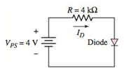
Figure 1.46 Circuit for exercise problem TYU 1.15. The diode can be cither a pn junction diode or a Schottky diode.
Want to see the full answer?
Check out a sample textbook solution
Chapter 1 Solutions
Microelectronics: Circuit Analysis and Design


- What is the difference between a diode and rectifier?arrow_forwardWhat is CEMF?arrow_forwardConsider the circuit shown in Figure 2. The cut-in voltage of each diode is . Let and assume both diodes are conducting. Determine if this is a valid assumption and explain your answer. And calculate the values of IR, ID, Ip2, and V.. Rj =1.7 kQ ww VB =1 V D1 Dz R2D 4 kQ Figure 2arrow_forward
- For a Silicon diode, the forward current is 109 times the reverse saturation current Is. What will be the value of the forward diode voltage? Assume eta to be 1.arrow_forwardProblem # 4 In the circuit shown below. Determine the following a. Vs (at the secondary) b. Vout (across RL) c. Vrip (ripple votage) d. VpC e. PIV (Peak Inverse Voltage) 10:1 Dy 1ISV ms Ouiput RL 2.2 k2 D, 50 pF All diodes are IN4001. alleeearrow_forwardTrue or False. Please explain. thank you As the temperature increases, the forward voltage decreases in a silicon diode. Then, the graph of the forward bias region will shift to the left.arrow_forward
- Calculate the current flowing through the given circuit and the voltage value at the V0 ends. (Threshold voltage = 0.3V for Germanium diodes, Threshold voltage for silicon diodes = 0.6V)arrow_forwardCompared to an ideal PN diode, what are the different characteristics of a practical PN diode? Please list two different characteristics when the diode is reversed biased.arrow_forwardConsider the diode circuit shown below. If Vs is a sinewave with a peak amplitude of 12 Volts at 60Hz, and diodes D1 & D2 are considered ideal, sketch the appearance of the waveform at node voltage Vout . Sketch the appearance of the waveform at Vout .arrow_forward
- When a conventional Silicon diode is reversed-biased with a voltage high enough such that there is a very large current present, the voltage value this occurs at is referred to as the: a) Breakdown voltage b) Breakup voltage c) Hammer voltage d) Roller voltage O b O d O c a o o o oarrow_forwardDetermine the value of RL that will establish maximum power conditions for the Zener diode.arrow_forward• A Si diode at a temperature of 25°C has VD = 0.7V at Is = 10nA. The temperature is raised to 125°C. 1. Calculate ID at 25°C. 2. What is effect of rise in temperature on VD & IS 3. Calculate ID at 125°C.arrow_forward

 Electricity for Refrigeration, Heating, and Air C...Mechanical EngineeringISBN:9781337399128Author:Russell E. SmithPublisher:Cengage Learning
 Delmar's Standard Textbook Of ElectricityElectrical EngineeringISBN:9781337900348Author:Stephen L. HermanPublisher:Cengage Learning